A NOT logic circuit, also known as an inverter, is one of the simplest yet most important digital logic circuits. It inverts the input signal: when the input is HIGH, the output is LOW, and vice versa. This post explains what a NOT logic circuit is, how it works, and how to build one using different technologies such as transistors, CMOS, and TTL.
Table of Contents
- What Is a NOT Logic Circuit?
- How Inverters Work in Logic Gates
- Transistor NOT Gate: How to Build One
- Circuit for NOT Gate Using CMOS Logic
- NOT Logic Circuit Applications
- Tips for NOT Logic Circuit Design
- Did You Know About the NOT Logic Circuit?
- Frequently Asked Questions About the NOT Logic Circuit
- What is a NOT gate in simple terms?
- How does a transistor create a NOT logic circuit?
- What are common ICs for NOT logic circuits?
- Can I make a NOT gate using only resistors?
- What happens if I connect two NOT gates in series?
- Why use a NOT gate instead of just flipping the signal in software?
- Are NOT gates used in memory circuits?
- What’s the difference between a NOT gate and a NAND gate?
- Conclusion on the NOT Logic Circuit
What Is a NOT Logic Circuit?
A NOT logic circuit performs logical inversion. It’s the hardware implementation of a NOT gate, which is one of the fundamental logic gates in digital electronics.
Beyond its simple function, the NOT logic circuit serves as the primary “decision-maker” for state changes in a system. In digital electronics, we operate in a binary world of 1s and 0s, which correspond to specific voltage levels. The NOT circuit is the active component responsible for flipping these states. Without the ability to invert a signal, we could never perform complex subtraction in binary or create timing signals, making this “simple” gate the literal backbone of logical processing.
From a physical perspective, the NOT logic circuit is an electronic amplifier configured to operate in saturation and cutoff modes. Unlike an analog amplifier that tries to replicate an input signal with more power, the NOT circuit purposefully drives the output to the opposite extreme of the input. This ensures that the digital signal remains crisp and clear, preventing undefined logic states where a voltage might sit somewhere between a 0 and a 1.
Truth Table for a NOT Gate
This simple truth table defines the entire behavior of a NOT gate circuit. It’s used in a wide range of digital designs, from microcontrollers to memory circuits. As the table below shows, the output logic level of the NOT gate is simply the opposite of the input logic level.
| Input (A) | Output (Y = NOT A) |
|---|---|
| 0 | 1 |
| 1 | 0 |
In Boolean algebra, the operation of a NOT logic circuit is often represented by a bar over the input variable (e.g., Y=A) or a prime symbol (A′). This mathematical notation is crucial when designing complex logic maps or simplifying circuit diagrams before they are physically built. Understanding how to read these symbols is a vital skill for any student of electronics, and you can find a deeper dive into this in our guide: NOT Gate Truth Table Made Easy: Logic Inverter Explained.
The simplicity of this table is what makes the NOT gate so reliable. Because there is only one input and one output, there is no ambiguity in the logic. If the input voltage meets the threshold for “High,” the output must drop to “Low.” This deterministic behavior allows engineers to use NOT gates to synchronize signals across different parts of a computer processor, ensuring that every component is on the same page at the exact same nanosecond.
How Inverters Work in Logic Gates
The inverter in logic gates works by producing the opposite logic state at the output. When implementing this behavior with components, we often use transistors or logic ICs.
At the silicon level, the inverter functions as a voltage-controlled switch. When a specific voltage threshold is reached at the input, the internal path between the output and the power supply is severed, while a path to the ground is opened. This transition must happen incredibly fast, often in picoseconds, to support the gigahertz speeds of modern computing. The efficiency of this “flip” determines how much heat a chip generates and how fast a device can run.
Examples
When looking for off-the-shelf components to experiment with, you will likely encounter Integrated Circuits (ICs) that house multiple inverters in a single package. These “Hex Inverters” are a staple of breadboard prototyping because they allow you to manage up to six different signals simultaneously with just one chip.
- In TTL logic, chips like the 7404 Hex Inverter contain six NOT gates.
- In CMOS logic, the CD4069 offers a similar function but with higher input impedance and lower power consumption.
Inverters are often the foundation of more complex logic circuits, such as oscillators, buffers, and even processors.
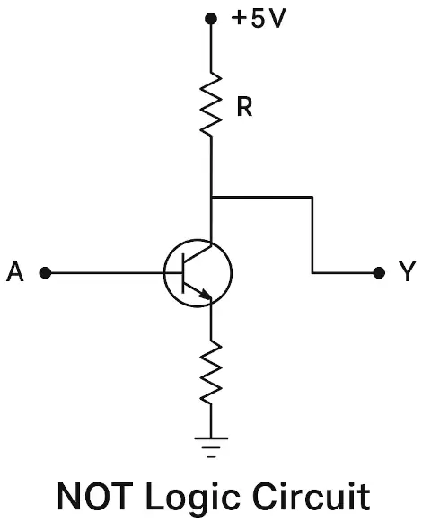
Transistor NOT Gate: How to Build One
A transistor NOT gate is the most basic form of a NOT logic gate circuit. Building a logic gate from discrete transistors is the best way to visualize how digital logic emerges from analog components. While modern computers use billions of microscopic transistors, the fundamental physics remains the same as the circuit you can build on a breadboard. By using a single NPN transistor, you can create a “Resistor-Transistor Logic” (RTL) gate, which was the same technology used in the Apollo Guidance Computer that went to the moon.
NPN Transistor Inverter Circuit
The NPN transistor inverter is a “common-emitter” configuration. In this setup, the transistor acts as a bridge to the ground. When you apply a small amount of current to the base, the bridge closes, and electricity takes the path of least resistance to the ground, leaving the output with no voltage.
Parts needed:
- NPN transistor (e.g., 2N3904 or BC547)
- Resistor (1kΩ–10kΩ)
- Power supply (5V)
How it works:
- Input is applied to the base via a resistor.
- When the input is HIGH, the transistor turns on, pulling the output LOW.
- When the input is LOW, the transistor is off, and the output is pulled HIGH via a pull-up resistor.
This is a simple, cost-effective way to demonstrate the behavior of a NOT gate.
Circuit for NOT Gate Using CMOS Logic
While the NPN transistor is great for learning, modern electronics almost exclusively use Complementary Metal-Oxide-Semiconductor (CMOS) logic. This technology uses a pair of transistors, one P-type and one N-type, working in tandem. The primary advantage here is efficiency: a CMOS inverter only draws significant power during the brief moment it is switching states. When it is sitting still at a 1 or a 0, it consumes almost zero energy, which is why your smartphone battery can last all day.
Basic CMOS Inverter
The CMOS inverter is considered “complementary” because the two transistors behave in opposite ways to the same input signal. This creates a push-pull effect that drives the output high or low very cleanly. The following are characteristics of a CMOS inverter.
- Made from a PMOS and NMOS transistor connected in series.
- The output is connected between them.
- When the input is HIGH, the PMOS turns OFF and NMOS turns ON, pulling the output LOW.
- When the input is LOW, the PMOS turns ON and NMOS turns OFF, pulling the output HIGH.
This configuration is at the heart of modern digital logic design, including processors and memory arrays.
NOT Logic Circuit Applications
The NOT logic circuit is far more than just a “signal flipper”; it is a versatile tool used to fix timing issues, clean up noisy signals, and even generate clock pulses. Because every digital operation eventually requires a state change, the applications of the inverter are found in almost every electronic device in your home. NOT gates are used in many real-world scenarios, such as the following.
- Signal inversion
- Oscillator design
- Pulse shaping
- Logic level conversion
- Buffering in high-impedance circuits
By combining NOT gates with other logic gates, you can create NAND, NOR, XOR, and more.
Tips for NOT Logic Circuit Design
Designing a reliable NOT logic circuit requires more than just connecting wires; you must account for real-world factors like electrical noise and “floating” inputs. A poorly designed inverter can lead to “glitches” where the circuit oscillates rapidly between states, potentially damaging sensitive downstream components or causing software errors. Take not of the following tips that will help when building circuits.
- Always use a pull-up resistor in transistor-based NOT gates.
- Use CMOS inverters for low-power applications.
- Debounce mechanical inputs before feeding them into NOT gates.
- Use buffer ICs like 74LS04 when driving higher loads.
- Simulate your circuit using logic simulation software before prototyping.
Did You Know About the NOT Logic Circuit?
The history and physics of the NOT gate are filled with surprising facts that highlight its importance in the evolution of technology. From the massive, glowing vacuum tubes of the 1940s to the 3-nanometer transistors of today, the inverter has shrunk in size by a factor of billions, yet its logical purpose hasn’t changed a bit.
- The first NOT gates were built using vacuum tubes before transistors existed.
- The CMOS inverter is the fundamental building block of nearly all modern digital ICs.
- You can use multiple NOT gates in series to create signal delays or oscillations.
- NOT gates are sometimes called inverting buffers, especially when used to drive signal lines.
Frequently Asked Questions About the NOT Logic Circuit
If you are new to digital logic, it is common to have questions about how such a simple gate can be so influential. Below, we have compiled comprehensive answers to the most common queries regarding the design, behavior, and implementation of logic inverters.
What is a NOT gate in simple terms?
In simple terms, a NOT gate is an “opposite-maker.” Imagine a light switch that turns the light off when you flip it up and on when you flip it down, that is exactly how a NOT gate behaves. It takes whatever signal it receives (High/1 or Low/0) and outputs the complete opposite. It is the digital equivalent of saying “No” to whatever the input says.
How does a transistor create a NOT logic circuit?
A transistor creates a NOT gate by acting as a controlled path to the ground. In an NPN setup, the output is connected to a power source through a resistor. When the input is “High,” the transistor activates and acts like a closed wire connecting the output directly to the ground (0V). This “shorts” the signal to the ground, resulting in a “Low” output. When the input is “Low,” the transistor is an open switch, so the electricity from the power source has nowhere to go but to the output, resulting in a “High” signal.
What are common ICs for NOT logic circuits?
The two most famous ICs are the 7404 (TTL) and the CD4069 (CMOS). The 7404 is part of the classic 7400-series logic and is known for its speed and ability to drive other gates, but it requires a strict 5V supply. The CD4069 is a CMOS version that is more flexible with voltage (often 3V to 15V) and draws much less power, making it ideal for battery-operated projects.
Can I make a NOT gate using only resistors?
No, you cannot. A resistor is a passive component; it can reduce current or divide voltage, but it cannot “switch” states based on an input. To create a NOT gate, you need an active component like a transistor or a vacuum tube that can change its internal resistance from “nearly zero” to “nearly infinite” in response to an external signal.
What happens if I connect two NOT gates in series?
Connecting two NOT gates in series creates what is known as a buffer. The first gate inverts the signal (1 becomes 0), and the second gate inverts it again (0 becomes 1), returning it to its original state. While this might seem useless, it is actually very helpful for strengthening a weak signal or adding a tiny “propagation delay” to help synchronize different parts of a fast-moving circuit.
Why use a NOT gate instead of just flipping the signal in software?
While software can easily flip a bit, it takes time for a processor to fetch an instruction, execute it, and update a pin. A hardware NOT gate works at the speed of light (almost), providing an instantaneous reaction. In high-speed applications like radio frequency (RF) processing or motor control safety interrupts, waiting for software is too slow, hardware logic ensures the system reacts in real-time.
Are NOT gates used in memory circuits?
Yes, NOT gates are a primary component of Static RAM (SRAM). By connecting two inverters in a loop (where the output of one feeds the input of the other), you create a “latch.” This loop can hold a single bit of data (a 1 or a 0) indefinitely as long as power is supplied. This is the foundation of the cache memory inside your computer’s CPU.
What’s the difference between a NOT gate and a NAND gate?
A NOT gate has only one input and always inverts it. A NAND gate (NOT-AND) has two or more inputs. A NAND gate only produces a “Low” output if all of its inputs are “High.” Interestingly, a NAND gate is considered a “Universal Gate” because if you tie both of its inputs together, it actually functions exactly like a NOT gate!
Conclusion on the NOT Logic Circuit
The NOT logic circuit is a core component in digital electronics. From simple transistor-based inverters to high-speed CMOS implementations, NOT gates are used in virtually every digital system. Understanding how to build and apply NOT logic circuits is a fundamental skill for any electronics enthusiast or engineer.
Whether you’re designing a basic project or diving into IC architecture, mastering the NOT logic gate circuit opens the door to more complex digital design.